


Automatic or automated optical inspection, AOI, is a key technique used in the manufacture and test of electronics printed circuit boards, PCBs. Automatic optical inspection, AOI enables fast and accurate inspection of electronics assemblies and in particular PCBs to ensure that the quality of product leaving the production line is high and the items are built correctly and without manufacturing faults.
Need for AOI, automatic optical inspection
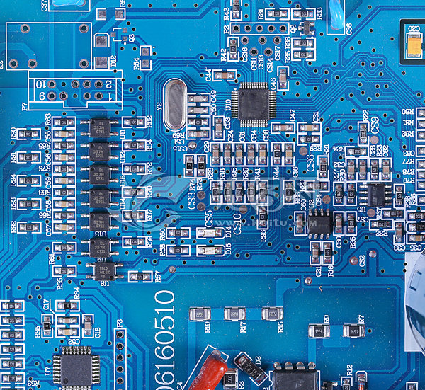
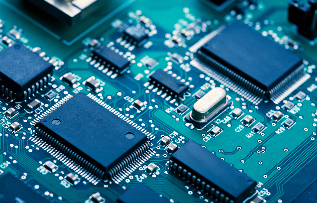
Despite the major improvements that have been made, modern circuits are far more complicated than boards were even a few years ago. The introduction of surface mount technology, and the subsequent further reductions in size mean that boards are particularly compact. Even relatively average boards have thousands of soldered joints, and these are where the majority of problems are found.
This increase in the complexity of boards also means that manual inspection is not a viable option these days. Even when it was an accepted approach, it was realised that it was not particularly effective as inspectors soon tired and poor and incorrect construction was easily missed. With the marketplace now requiring high volume, high quality products to be brought to market very quickly very reliable and fast methods are needed to ensure that product quality remains high. AOI, automatic optical inspection is an essential tool in an integrated electronics test strategy that ensure costs are kept as low as possible by detecting faults early in the production line.
One of the solutions to this is to use automated or automatic optical inspection systems. Automated optical inspection systems can be placed into the production line just after the solder process. In this way they can be used to catch problems early in the production process. This has a number of advantages. With faults costing more to fix the further along the production process they are found, this is obviously the optimum place to find faults. Additionally process problems in the solder and assembly area can be seen early in the production process and information used to feedback quickly to earlier stages. In this way a rapid response can ensure that problems are recognised quickly and rectified before too many boards are built with the same problem.
| COMPARISON OF THE MAJOR DEFECT DETECTION CAPABILITIES OF AOI, AXI AND ICT | |||
|---|---|---|---|
| DEFECT TYPE | AOI | AXI | ICT |
| Soldering defects | |||
| Open circuits | Y | Y | Y |
| Solder bridges | Y | Y | Y |
| Solder shorts | Y | Y | Y |
| Insufficient solder | Y (not heel of joint) | Y | N |
| Solder void | N | Y | N |
| Excess solder | Y | Y | N |
| Solder quality | N | Y | N |
| Component defects | |||
| Lifted lead | Y | Y | Y |
| Missing component | Y | Y | Y |
| Misaligned or misplaced component | Y | Y | Y |
| Incorrect component value | N | N | Y |
| Faulty component | N | N | Y |
| BGA and CSP defects | |||
| BGA shorts | N | Y | Y |
| BGA open circuit connections | N | Y | Y |
AOI, automatic optical inspection basics
AOI, automatic optical inspection systems use visual methods to monitor printed circuit boards for defects. They are able to detect a variety of surface feature defects such as nodules, scratches and stains as well as the more familiar dimensional defects such as open circuits, shorts and thinning of the solder. They can also detect incorrect components, missing components and incorrectly placed components. As such they are able to perform all the visual checks performed previously by manual operators, and far more swiftly and accurately.
They achieve this by visually scanning the surface of the board. The board is light by several light sources and one or more high definition cameras are used. In this way the AOI machine is able to build up a picture of the board
The automated optical inspection, AOI system uses the captured image which is processed and then compared with the knowledge the machine has of what the board should look like. Using this comparison the AOI system is able to detect and highlight any defects or suspect areas.
AOI uses a number of techniques to provide the analysis of whether a board is satisfactory or has any defects:
Template matching: Using this form of process the AOI, automated optical inspection system compares the image obtained with the image from a “golden board”.
Pattern matching: Using this techniques the AOI system stores information of both good and bad PCB assemblies, matching the obtained image to these.
Statistical pattern matching: This approach is very similar tot hat above, except that it uses a statistically based method of addressing problems. By storing the results of several boards and several types of failure, it is able to accommodate minor acceptable deviations without flagging errors.
In order to build up the database of what the board should be, both known status boards and PCB design information is used as described later.
As technology has improved it has been able for AOI systems to very accurately predict defects and have a small number of no defect found scenarios. As such AOI systems form a very useful element in a sophisticated manufacturing environment.
AOI image capture and analysis
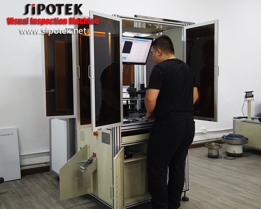
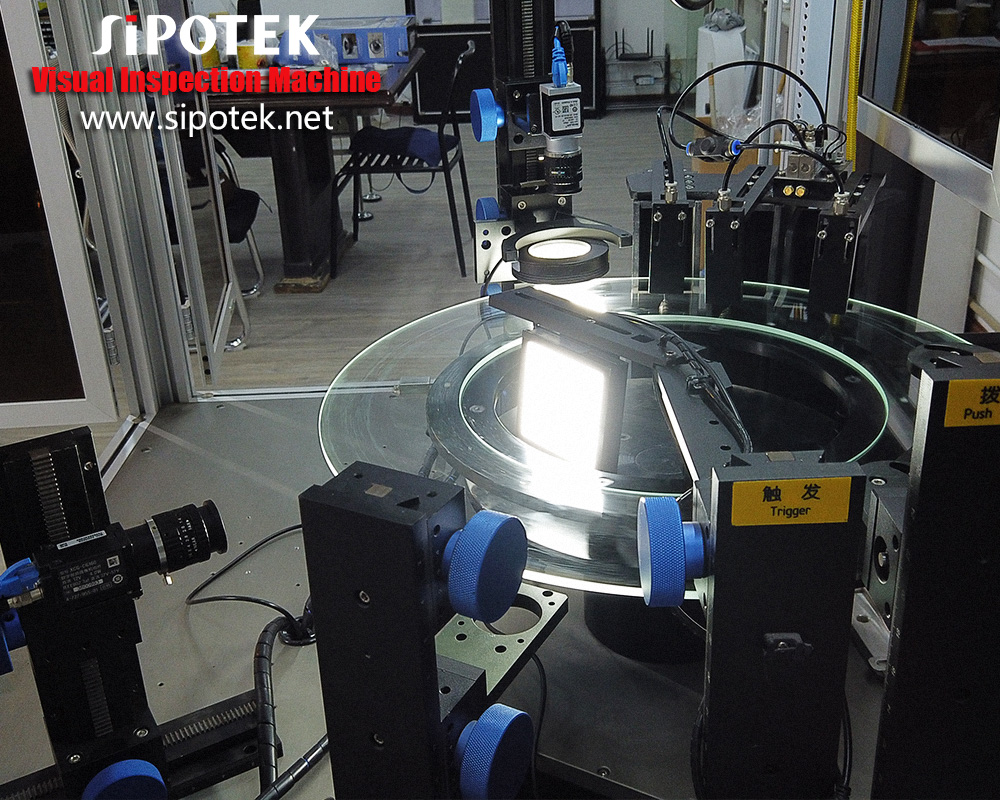
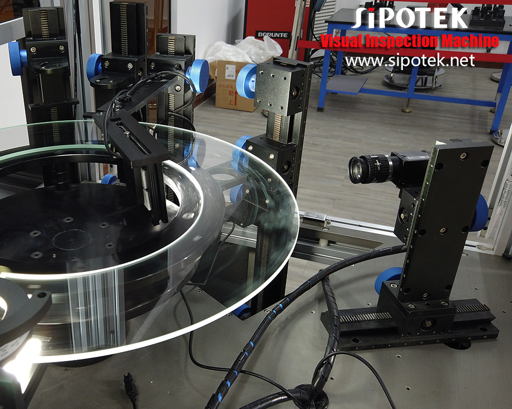
One of the key elements of an AOI, automated optical inspection system is the image capture system. This captures an image of the printed circuit board, PCB assembly which is then analysed by the processing software within the AOI system. There are many variants of image capture system dependent upon the exact application and the complexity / cost of the AOI system.
Imaging systems may comprise a single camera or there may be more than one to provide better imaging and the possibility of a 3D capability. The cameras should also be able to move under software control. This will enable them to move to the optimum position for a given PCB assembly.
In addition to this the type of camera has an impact on performance. Speed against accuracy is a balance that has to be struck and will impact on the camera type used:
Streaming video: One type of camera used for automated optical inspection, AOI, takes streaming video from which complete frames are taken. The captured frame then enables a still image to be generated on which the signal processing is performed. This approach is not as accurate as other still image systems but has the advantage of very high speed.
Still image camera system: This is generally placed relatively close to the target PCB and as a result it requires a good lighting system. It may also be necessary to be able to move the camera under software control.
When analysing an image of a board, the AOI system looks for a variety of specific features: component placement, component size, board fiducials, label patterns (e.g. bar codes), background colour and reflectivity, etc. As an important element of its task the AOI system also inspects the soldered joints to ensure they indicate that the joints are satisfactory.
When analysing the boards the AOI system must take into account many variations between good boards. Not only do components vary considerably in size between batches, but also the colour and reflectivity. Often there are also differences in the silk screening where ink thickness and colour typeface may change slightly.
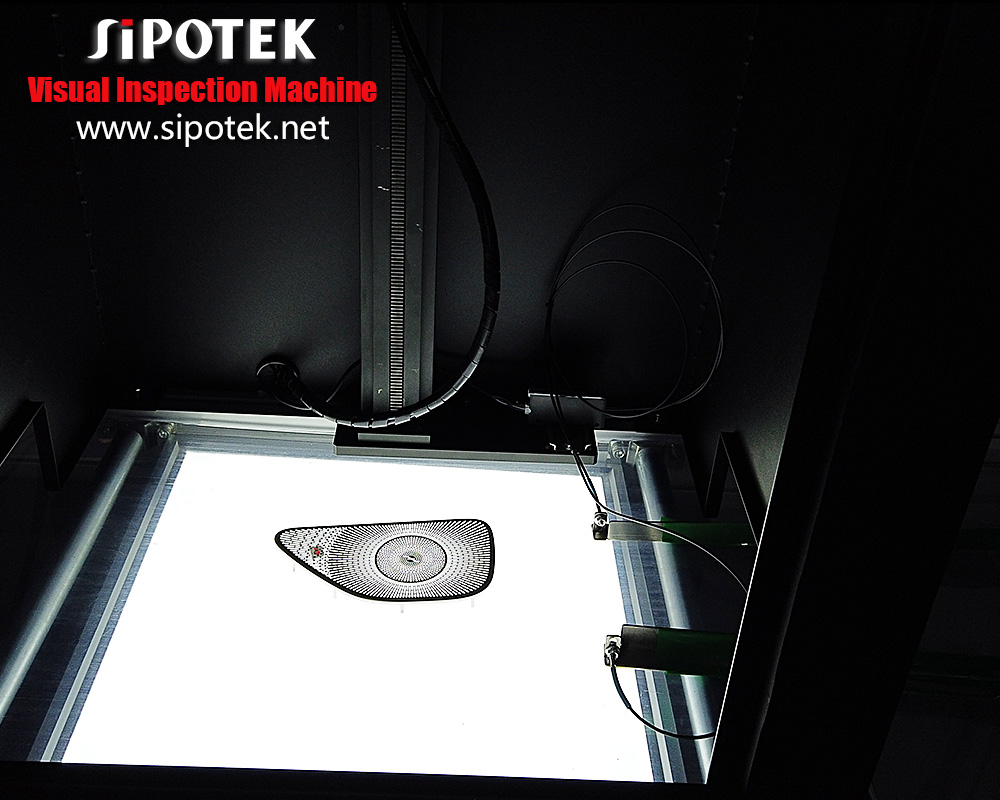
AOI light source
Lighting is a key element in the AOI system. By choosing the correct lighting source it is possible to highlight different types of defect more easily. With the advances that have been made in lighting technology in recent years, this has enabled lighting to be used to enhance the images available and in turn this enables defects to be highlighted more easily with a resultant reduction in processing required and an increase in speed and accuracy.
Most AOI systems have a defined lighting set. This will depend upon the operation required and the product types to be tested. These have usually been optimised for the anticipated conditions. However sometimes some customisation may be required, and an understanding of lighting is always of use.
A variety of types of lighting are available:
Fluorescent lighting: Fluorescent lighting is widely used for AOI, automated optical inspection applications as it provides an effective form of lighting for viewing defects on PCBs. The main problem with fluorescent lighting for AOI applications is that the lamps degrade with time. This means that the automated optical inspection system will be subject to a constantly changing levels and quality of light
LED lighting: The development of LED lighting has meant that AOI, automated optical inspection systems are able to adopt a far more stable form of lighting. Although LED lighting does suffer from a reduction in light output from the LEDs over time, this can be compensated for by increasing the current. Using LED lighting, the level of lighting can also be controlled. LEDs are therefore a far more satisfactory form of lighting than fluorescent or incandescent lights that were used years ago
Infra-red or ultra-violet: On some occasions infra-red or ultra-violet lighting may be required to enhance certain defects, or to enable automated optical inspection to be carried out to reveal certain types of defect.
Apart from the form of lighting, the positioning of the lighting for an automatic optical inspection system, AOI, is equally important. The light sources require positioning to not only to ensure that all areas are well light, which is particularly important when certain components may cast shadows, but also to highlight defects. Careful adjustment may be needed for different assemblies.
AOI, automated optical inspection system programming
In order to be able to test a PCB assembly using AOI, automatic optical inspection, the details for an acceptable board must be stored within the system. This programming activity must be carried out correctly if the AOI system is to be able to correctly detect any defects on the PCB assemblies passing through.
there are several methods that can be used to programme an AOI system:
Use of “Golden Board”: One method is to provide a known good board as a target for the AOI, automated optical inspection system to use. This is passed through the system so that it can learn the relevant attributes. It will look at the components, the solder profiles of each joint, and many other aspects. In order to provide the system with enough variance data several boards are often required.
Algorithm based programming: PCB data is provided to the system and it then generates its own profile for the board. This scheme will also require real boards, but fewer are generally required.
There are advantages and disadvantages to both systems. It is a balance between set-up time, maintenance, accuracy and the requirements for the particular AOI, automated optical inspection system. Typically the requirements will be largely dependent upon the machine in use.
It is essential that any printed circuit board manufacturing area is able to check the quality of the boards coming off the end of the line. Only in this way are they able to monitor quality and when problems are detected to rectify the process so that further boards are not affected by the same problems. In this way automatic optical inspection and where necessary X-ray inspection are two essential tools for the manufacturing industry.